One Package, 61% Smaller | Corezzle Electronics
Generative Hardware, SiP, Edge AI & IoT Solutions
One Package, 61% Smaller | Corezzle Electronics
One Package, 61% Smaller: The Board Area and Supply Chain Arithmetic
Every component on a board creates cost in three separate places. It occupies board area, it opens a line in the bill of materials, and it adds at least two solder joints on the assembly line. Taken one at a time, these costs are small. Added up across hundreds of components, they determine the size of your product, its unit cost and its field failure rate.
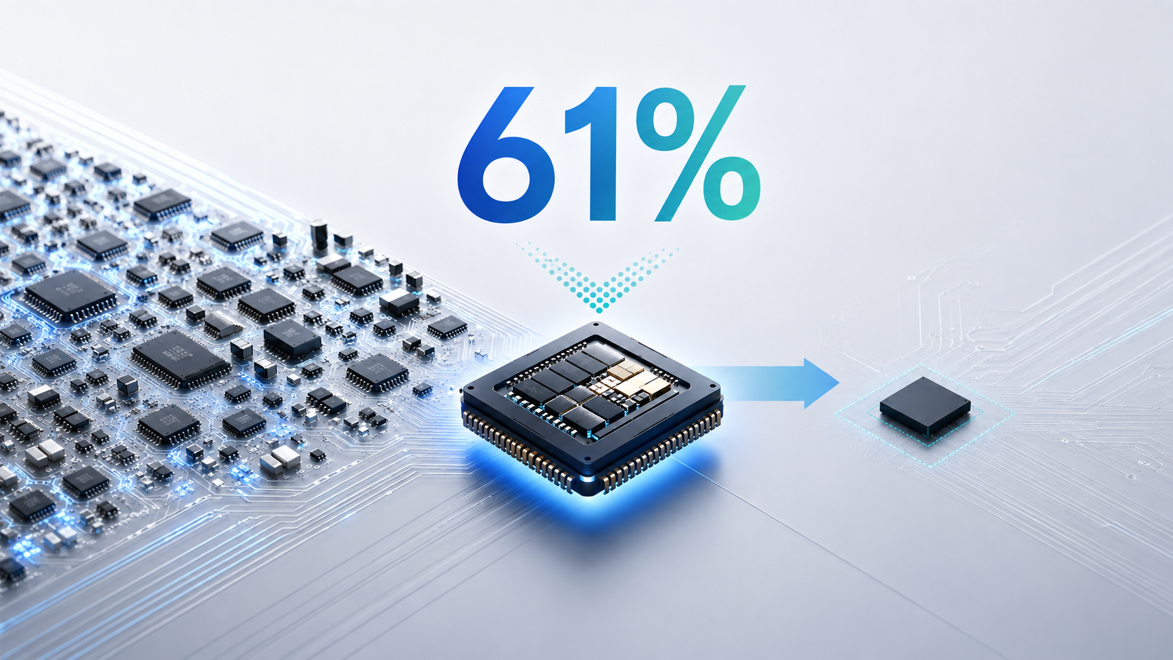
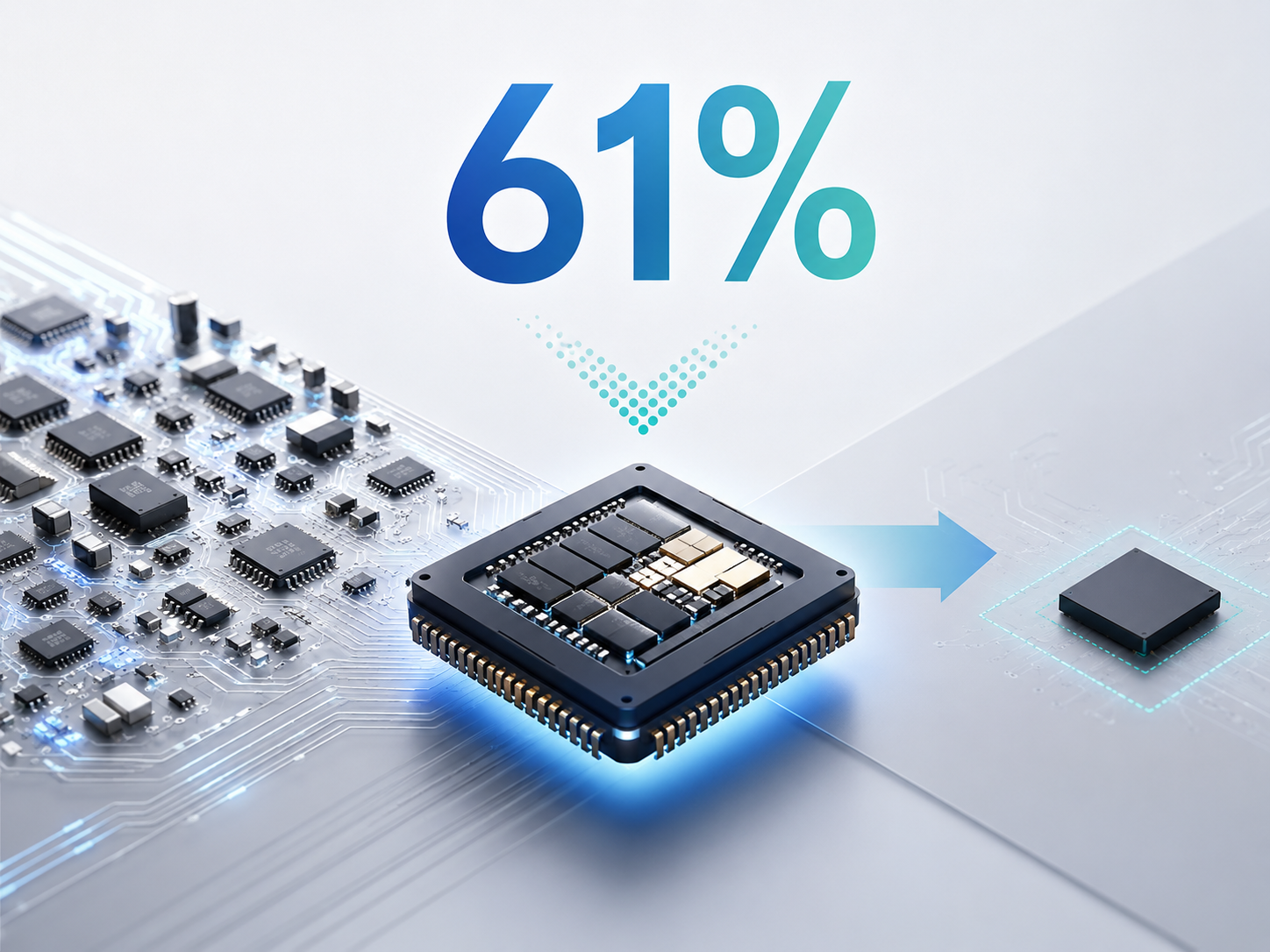
That arithmetic is the starting point of Nar Series System-in-Package (SiP) products. When the processor, memory, power management and communication components come together in a single package, the result is up to 61% board area savings. This post looks at where that number comes from and what else it brings along.
What goes into the package?
Concrete is best. Inside NAR-ESP32S3R16-32 you will find an ESP32-S3 microcontroller (including 16 MB PSRAM), 32 MB of QSPI flash, an AXP2101 power management IC, an ES8311 audio codec, an ES7210 four channel microphone converter, an ICM-42686-P six axis inertial measurement unit, a PCF85063 real time clock, USB-C surge protection and two separate crystals.
In a traditional design, every line on that list brings along its own supply separation, its own bypass capacitors and its own placement rules. The active component count passes twenty, and with passives the total climbs much higher.
The picture on the NAR-3358 side is similar: a TI Sitara AM3358 processor, DDR3L memory, eMMC storage, two separate power management ICs, an EEPROM for board identity, a reset buffer and the clock crystals all sit in one package. In a traditional AM335x design that block corresponds to more than 100 active and passive components. With Nar Series it stands in your schematic as a single symbol.
Where does the 61% go?
The board area gain does not come only from the footprints of the components. The real gain comes from the distances between them and from the routing corridors they demand.
A high speed memory bus needs serpentine area for length matching. Power rails need wide copper between converters and loads. Analog blocks want distance from noisy digital ones. On the board, all of this takes up more room than the component footprints themselves.
Moving those paths inside the package produces three results at once. Board area shrinks, layer count drops and the assembly step gets simpler. Fewer solder joints on the board also pays off in reliability, because a significant share of field failures from mechanical and thermal fatigue starts at solder joints.
One line item in the supply chain
Board area is only the visible side of this arithmetic. What happens on the purchasing side matters just as much.
In a traditional design, every line in the bill of materials is a tracking job of its own. Each component has its own lead time, its own minimum order quantity and its own list of alternates. On top of that comes the chance of it going out of production: one day the manufacturer issues an end-of-life notice for that part, and you have to find a replacement and revisit the board. When a single line on that list runs into trouble, the whole product waits. With Nar Series, that entire block comes down to a single part number. You track one line item instead of dozens, and the burden of component selection, lifecycle management and second sourcing stays with us.
Manufacturing sees a similar simplification. The dies inside the package may carry different moisture sensitivity levels, but the SiP is documented against a single one. For NAR-ESP32S3R16-32 that level is MSL3 with a 260 °C peak. On the assembly line, the tolerances of dozens of separate parts are not worked out one by one; a single profile is applied. The product is supplied in both tape and reel and tray formats, so it drops straight into your existing assembly line.
The package type is a deliberate choice
Making something smaller does not have to make manufacturing harder. In NAR-ESP32S3R16-32 a castellated LGA (Land Grid Array) package is used. Because the pads along the side edges are half-moon shaped, the solder fillet can be inspected visually after reflow and reworked by hand when needed. During prototyping and low volume production, that is a clear advantage over packages with hidden connections.
For NAR-3358, which needs a high pin count, a BGA package is used. The package type is selected per product according to the number of connections and the intended manufacturing scenario: a castellated LGA when the connections fit along the edges and easy hand soldering matters, a BGA using the whole underside of the package when many more connections are needed.
What shrinking means for the product
When the board shrinks, product design gets easier. A wearable enclosure gets thinner, a sensor node makes room for a bigger battery, an industrial controller fits more I/O into the same rail width. In some products the gain lands directly on cost, because a smaller board means fewer layers and a smaller enclosure.
So 61% is not a marketing figure on its own. It opens room you can actually use in your product design.
Contact: [email protected]
Featured Posts
Months Turn Into Days | Corezzle Electronics
2026-08-10
Does Hardware Development Really Have to Be This Complex?
2026-04-08Recently Added Posts
One Package, 61% Smaller | Corezzle Electronics
2026-08-10
We Take On the Risk | Corezzle Electronics
2026-08-10